Inverse Design: Grating Coupler
End-to-end topology optimization of a 220nm SOI grating coupler, from freeform optimization through fabrication-ready GDS export.
Note: This is an interactive walkthrough of our inverse design pipeline, not a runnable notebook. The code cells below illustrate the workflow and API, and the outputs shown are real results from actual optimization runs. The underlying optimization engine, binarization methods, and fabrication constraint solvers are proprietary. To run inverse design on your own devices, contact us for API access.
What you will learn
- 1.Set up a grating coupler inverse design problem on 220nm SOI
- 2.Run freeform topology optimization with adjoint gradients
- 3.Apply binarization and fabrication constraints for manufacturability
- 4.Verify DRC compliance and export to GDSII
Environment Setup
This tutorial walks through the inverse design of a 220nm SOI grating coupler optimized for 1550nm TE-polarized light. You will define the device, run a multi-stage optimization pipeline (freeform, binarization, DFM cleanup), and export a foundry-ready GDS layout.
The optimization schedules (learning rates, projection ramps, constraint weights, phase transitions) shown in this tutorial have been simplified. The actual schedules used to produce these results are proprietary. As an API user, you have full control over all schedule parameters and can customize every aspect of the optimization pipeline for your own devices.
You'll need a Hyperwave API key. Sign up at spinsphotonics.com/signup to get one.
# Install dependencies
!pip install -q hyperwave-community matplotlib

# Imports
import numpy as np
import hyperwave_community as hwcDevice Configuration
We target a standard 220nm silicon-on-insulator platform with a 110nm partial etch, operating at 1550nm. The grating coupler accepts light from a single-mode fiber (SMF-28) tilted at 14.5 degrees and routes it into a 500nm-wide strip waveguide.
All parameters match standard silicon photonics foundry processes (AIM, GlobalFoundries 45SPCLO). The 110nm partial etch is the most common etch depth for grating couplers on 220nm SOI.
All feature sizes in this pipeline are set in integer pixel units. The density filter uses a conic kernel of radius R pixels, giving a minimum feature size of (2R+1) * pixel_size. DRC checks use morphological opening with a disk of radius r pixels, checking for features smaller than (2r+1) * pixel_size. There is no sub-pixel precision: what you see is what the foundry gets.
# --- Material refractive indices ---
n_si = 3.48          # Silicon at 1550nm
n_sio2 = 1.44        # SiO2 cladding
n_air = 1.0          # Air / top cladding

# --- Wavelength and grid ---
wavelength = 1.55    # um (1550nm)
fdtd_grid = 0.035    # um (35nm FDTD grid spacing)
theta_grid = fdtd_grid / 2  # 17.5nm design grid (2x oversampling)

# --- Device stack ---
wg_height = 0.220    # um (full silicon thickness)
etch_depth = 0.110   # um (partial etch for grating)
slab_height = wg_height - etch_depth  # 110nm remaining slab
box_thickness = 2.0  # um (buried oxide)
clad_thickness = 2.0 # um (top cladding)

# --- Waveguide ---
wg_width = 0.500     # um (single-mode strip waveguide)

# --- Fiber parameters ---
fiber_angle = 14.5   # degrees from surface normal
beam_waist = 5.2     # um (SMF-28 mode field diameter / 2)

# --- Design region ---
design_length = 35.0 # um (grating coupler length)
design_width = 35.0  # um (grating coupler width)

# --- Feature size constraints (integer pixel units) ---
# density_radius is set per design layer when calling hwc.density()
# R=6 pixels -> min feature = (2*6+1) * 17.5nm = 228nm
drc_disk_radius = 3          # disk(r=3), DRC check = (2*3+1)*17.5nm = 122nm

print(f"Device: {int(wg_height*1000)}nm SOI, {int(etch_depth*1000)}nm etch, {int(wavelength*1000)}nm")
print(f"Grid: {int(fdtd_grid*1000)}nm FDTD, {theta_grid*1000:.1f}nm theta")
print(f"Density filter: R=6 -> min feature = {(2*6+1)*theta_grid*1000:.0f}nm (set per-layer)")
print(f"DRC disk: r={drc_disk_radius} -> min check = {(2*drc_disk_radius+1)*theta_grid*1000:.0f}nm")Layer Stack
The SOI layer stack follows the standard pipeline: define layers as Layer objects with density patterns and permittivity values, then assemble them with create_structure(). Design layers use the conic density filter (hwc.density()) to enforce minimum feature sizes. The two design layers (etch and slab) are where the optimizer will place or remove material.
# --- Grid dimensions ---
nx = int(design_length / theta_grid)   # x pixels (propagation direction)
ny = int(design_width / theta_grid)    # y pixels (transverse direction)

print(f"Grid: {nx} x {ny} pixels ({design_length} x {design_width} um)")

# --- Layer stack definition ---
layers = [
    {"name": "substrate", "thickness": 0.5, "index": n_si},
    {"name": "box", "thickness": box_thickness - 0.5, "index": n_sio2},
    {"name": "slab", "thickness": slab_height, "index": n_si,
     "design": True, "density_radius": 6, "initial_value": 1.0},
    {"name": "etch", "thickness": etch_depth, "index": n_si,
     "design": True, "density_radius": 6, "initial_value": 0.5,
     "waveguide_width": wg_width},
    {"name": "clad_lower", "thickness": 0.5, "index": n_sio2},
    {"name": "clad_upper", "thickness": clad_thickness - 0.5, "index": n_sio2},
    {"name": "air_gap", "thickness": 0.3, "index": n_air},
    {"name": "air", "thickness": 0.2, "index": n_air},
]

# --- Initialize theta (design variables) ---
import jax.numpy as jnp
theta_slab = jnp.ones((nx, ny), dtype=jnp.float32)   # slab: solid silicon
theta_etch = jnp.full((nx, ny), 0.5, dtype=jnp.float32)  # etch: grayscale start

# --- Apply density filter to see physical density ---
density_slab = hwc.density(theta_slab, radius=6)
density_etch = hwc.density(theta_etch, radius=6)

# --- Build Layer objects ---
h_slab = int(round(slab_height / fdtd_grid))
h_etch = int(round(etch_depth / fdtd_grid))

slab_layer = hwc.Layer(density_slab, permittivity_values=(n_sio2**2, n_si**2), layer_thickness=h_slab)
etch_layer = hwc.Layer(density_etch, permittivity_values=(1.0, n_si**2), layer_thickness=h_etch)

# Non-design layers (fixed permittivity)
substrate_layer = hwc.Layer(jnp.zeros((nx, ny)), permittivity_values=n_si**2, layer_thickness=int(0.5/fdtd_grid))
box_layer = hwc.Layer(jnp.zeros((nx, ny)), permittivity_values=n_sio2**2, layer_thickness=int((box_thickness-0.5)/fdtd_grid))
clad_lower_layer = hwc.Layer(jnp.zeros((nx, ny)), permittivity_values=n_sio2**2, layer_thickness=int(0.5/fdtd_grid))
clad_upper_layer = hwc.Layer(jnp.zeros((nx, ny)), permittivity_values=n_sio2**2, layer_thickness=int((clad_thickness-0.5)/fdtd_grid))
air_gap_layer = hwc.Layer(jnp.zeros((nx, ny)), permittivity_values=n_air**2, layer_thickness=int(0.3/fdtd_grid))
air_layer = hwc.Layer(jnp.zeros((nx, ny)), permittivity_values=n_air**2, layer_thickness=int(0.2/fdtd_grid))

# --- Assemble structure ---
structure = hwc.create_structure(
    layers=[substrate_layer, box_layer, slab_layer, etch_layer,
            clad_lower_layer, clad_upper_layer, air_gap_layer, air_layer],
)

Lx, Ly, Lz = structure.permittivity.shape[1], structure.permittivity.shape[2], structure.permittivity.shape[3]
print(f"Structure shape: ({Lx}, {Ly}, {Lz})")
print(f"Design layers: slab (h={h_slab}px), etch (h={h_etch}px)")

# Visualize the layer stack (XZ cross-section)
hwc.plot_structure(structure)Cost Estimate
Each optimization step requires two FDTD simulations: one forward pass and one adjoint pass. The cost per step is straightforward: simulation volume times timesteps, divided by GPU throughput, times two.
The ~537s estimate is pure FDTD compute. Actual wall time is ~604s/step due to gradient computation, checkpointing, and I/O overhead. We used 20,000 timesteps for this device (large domain, need full field stabilization), but this is configurable. Hyperwave also supports an auto-convergence mode that stops early when the fields have settled, which can significantly reduce cost for smaller devices.
# --- Cost estimate ---
# FDTD volume (from structure dimensions)
N_cells = Lx * Ly * Lz
timesteps = 20000         # FDTD timesteps per simulation (manual, for stability)
gcups = 30                # Hyperwave throughput: 30 billion cell-updates/sec

sim_time = N_cells * timesteps / (gcups * 1e9)  # seconds per simulation
step_time = sim_time * 2  # forward + adjoint per optimization step

print(f"Cost estimate:")
print(f"  FDTD volume:  {Lx} x {Ly} x {Lz} = {N_cells:,.0f} cells")
print(f"  Timesteps:    {timesteps:,} per simulation")
print(f"  Throughput:   {gcups} GCUPs")
print(f"  Per sim:      {N_cells:,.0f} * {timesteps:,} / {gcups}e9 = {sim_time:.0f}s")
print(f"  Per step:     {sim_time:.0f}s * 2 (fwd + adj) = {step_time:.0f}s (~{step_time/60:.0f} min)")
print(f" Full pipeline (~400 steps): ~{step_time * 400 / 3600:.0f} GPU-hours")Design Region
The design region is defined by the theta arrays we initialized earlier. Each design layer starts with an initial theta value (0 = void, 0.5 = grayscale, 1 = solid). The density filter hwc.density(theta, radius) converts theta to physical density. Here we add a waveguide taper to the etch layer's theta.
The etch layer starts at 0.5 (grayscale) to give the optimizer freedom to push pixels toward either silicon or air. The slab layer stays solid (1.0) throughout optimization.
# --- Initialize design region ---
# theta shape: (num_design_layers, nx, ny)
# Layer 0 = slab (fixed at 1.0), Layer 1 = etch (optimizable)
theta = np.zeros((2, nx, ny))
theta[0, :, :] = 1.0   # Slab layer: solid silicon everywhere
theta[1, :, :] = 0.5   # Etch layer: start at midpoint (grayscale)

# Add waveguide taper at output edge
taper_length = int(3.0 / theta_grid)  # 3um taper
taper_width_start = int(wg_width / theta_grid)
taper_width_end = int(12.0 / theta_grid)  # 12um grating width

for i in range(taper_length):
    frac = i / taper_length
    w = int(taper_width_start + frac * (taper_width_end - taper_width_start))
    y_start = ny // 2 - w // 2
    y_end = ny // 2 + w // 2
    theta[1, i, y_start:y_end] = 1.0  # Solid in taper region

print(f"Design region: {design_length} x {design_width} um")
print(f"Design pixels: {nx * ny:,}")
print(f"Etch layer initialized to 0.5 (grayscale)")

# Visualize the initial theta (etch layer)
hwc.plot_theta(theta[1])Gaussian Source
The source is a tilted Gaussian beam that models the fiber output. The beam parameters match SMF-28 single-mode fiber: 5.2um beam waist at 1550nm, incident at 14.5 degrees from the surface normal. Hyperwave generates the full 2D field profile and calculates input power for coupling efficiency normalization.
# Generate tilted Gaussian beam (SMF-28 fiber, 14.5 degree angle)
Lx, Ly, Lz = device.shape
freq = device.freq_band[0]
source_x = Lx // 2               # center of domain
source_y = Ly // 2
source_z = Lz - 30               # near top surface

source_field, input_power = hwc.generate_gaussian_source(
    sim_shape=device.shape,
    frequencies=np.array([freq]),
    source_pos=(source_x, source_y, source_z),
    waist_radius=int(beam_waist / fdtd_grid),   # 5.2um / 35nm = 149 pixels
    theta=fiber_angle * np.pi / 180,             # 14.5 deg in radians
    polarization='y',                             # TE polarization
    wavelength_um=wavelength,
    dx_um=fdtd_grid,
    gpu_type="B200",
)
print(f"Source generated. Input power: {float(input_power):.2f}")
print(f"Source field shape: {source_field.shape}")

# Visualize source field
import matplotlib.pyplot as plt
fig, (ax1, ax2) = plt.subplots(1, 2, figsize=(12, 5))
mid_z = source_field.shape[4] // 2
ax1.imshow(np.abs(source_field[0, 1, :, :, mid_z])**2)
ax1.set_title("|Ey|^2 (XY plane)")
mid_y = source_field.shape[3] // 2
ax2.imshow(np.real(source_field[0, 1, :, mid_y, :]).T, aspect="auto")
ax2.set_title("Re(Ey) (XZ plane)")
plt.tight_layout()
plt.show()Waveguide Mode
The optimization objective is to maximize the overlap between the guided mode and the field at the waveguide output. We solve for the TE0 fundamental mode of the 500nm x 220nm silicon strip waveguide. The effective index and mode profile are used to compute coupling efficiency at each optimization step.
# Solve TE0 fundamental mode of 500nm x 220nm Si waveguide
mode_field, n_eff = hwc.solve_waveguide_mode(
    grid=fdtd_grid,
    waveguide_width=wg_width,     # 0.5 um
    waveguide_height=wg_height,   # 0.220 um
    n_core=n_si,
    n_clad=n_sio2,
    wavelength=wavelength,
    mode_number=0,                # fundamental TE
)
print(f"TE0 effective index: {n_eff:.4f}")
print(f"Mode confinement: n_eff > n_clad ({n_eff:.4f} > {n_sio2})")

# Visualize the waveguide mode
hwc.plot_mode(mode_field, beta=n_eff, mode_num=0)Objective Function
The optimizer needs a scalar objective to maximize. For a grating coupler, this is the mode coupling efficiency: the fraction of input power that couples into the target waveguide mode.
At each step, the FDTD simulation produces the output field (E_sim, H_sim) at the waveguide monitor plane. We compute the modal transmission T using the product of two cross-product overlap integrals with the reference mode (E_m, H_m):
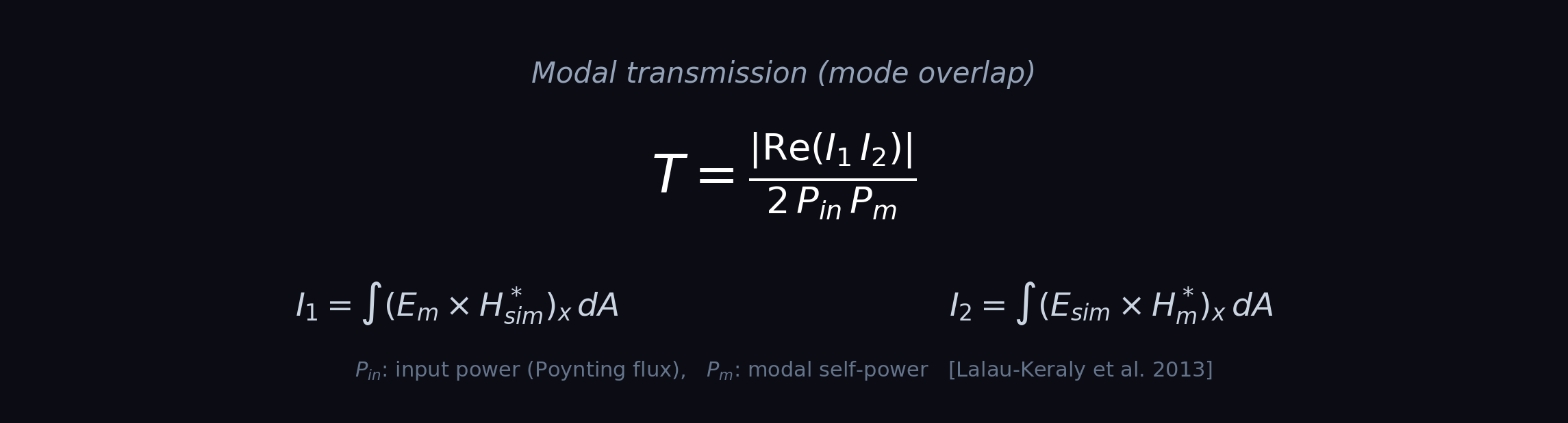
P_in is the input power measured from a Poynting-flux calibration monitor downstream of the source, and P_m is the modal self-power. This product formulation, building on Lalau-Keraly et al. 2013, uses explicit P_in and P_m factors that are robust to mode-solver normalization conventions and yield correct gradients without manual mode-power bookkeeping. When the simulated field perfectly matches the target mode, T = 1.
The adjoint method computes the gradient of this objective with respect to every design pixel in a single backward simulation, making it feasible to optimize millions of parameters simultaneously.
Objectives are expression trees built with operator overloading. They serialize to JSON and are evaluated on the GPU with full JAX autodiff support. No user code runs on the GPU, which makes this safe for multi-tenant cloud execution. You can compose any differentiable objective from the provided primitives: mode coupling, power flow, field intensity, and spatial reductions.
# Define the optimization objective using expression trees
# Mode coupling: maximize overlap with the target waveguide mode
objective = hwc.objectives.mode_coupling(
    mode_field=mode_field,
    input_power=float(input_power),
    mode_cross_power=1.0,            # mode self-overlap power
    monitor="waveguide_output",
)

# Expression trees compose with standard math operators:
# Broadband: maximize worst-case across wavelengths
# e1 = hwc.objectives.mode_coupling(mode_field, P_in, P_m, "wg", freq_idx=0)
# e2 = hwc.objectives.mode_coupling(mode_field, P_in, P_m, "wg", freq_idx=1)
# e3 = hwc.objectives.mode_coupling(mode_field, P_in, P_m, "wg", freq_idx=2)
# objective = hwc.objectives.min_of(e1, e2, e3)

# Field-level objectives:
# ey = hwc.objectives.field("Ey", "focus_monitor")
# objective = hwc.objectives.sum_spatial(hwc.objectives.abs_val(ey))

print(f"Objective: mode coupling efficiency")
print(f"Type: {type(objective).__name__}")Phase 1: Freeform Optimization
Unconstrained topology optimization using the adjoint method. Gradients are computed through the full 3D FDTD simulation automatically. The density filter radius (R=6, set per design layer) regularizes the design and sets the minimum feature size.
Each optimization step runs a forward and adjoint simulation on the cloud. For this device (1142 x 1142 x 309 voxels), each step takes approximately 10 minutes. Results are checkpointed at every step, so you can stop a run at any point and resume from where you left off.
# Phase 1: Freeform topology optimization
# Request up to 100 steps. We can stop the run early if efficiency plateaus.
results_freeform = hwc.optimize(
    layers=layers,
    theta={"slab": theta_slab, "etch": theta_etch},
    grid=fdtd_grid,
    wavelength=wavelength,
    source=source_field,
    mode=mode_field,
    phase="freeform",
    n_steps=100,
)

# Plot results
hwc.plot_phase_summary(results_freeform, title="Freeform", show_fields=True)
We requested 100 steps but stopped the run at step 61 once we saw efficiency plateau around 76.8%. The freeform design achieves high efficiency but contains continuous (grayscale) density values that cannot be directly fabricated. The next phases convert this to a binary, manufacturable design.
Phase 2: Binarization
Progressive binarization pushes the continuous design toward binary (0 or 1) values using Heaviside projection. You control the projection sharpness via beta_init and beta_max. Two common strategies:
A single call with beta_init=4, beta_max=64 linearly ramps sharpness over N steps. Simple and effective for most devices.
Multiple calls at fixed beta values (8, 16, 32, 64), each for a set number of steps. The optimizer stabilizes at each sharpness level before increasing. More conservative, can help when continuous ramping causes instability.
# Strategy A: Continuous ramp (used here for the GC)
results_binarize = hwc.optimize(
    layers=layers,
    grid=fdtd_grid,
    wavelength=wavelength,
    initial_design=results_freeform.design,
    source=source_field,
    mode=mode_field,
    phase="binarize",
    n_steps=200,
    beta_init=4.0,        # start soft
    beta_max=64.0,        # end sharp
    learning_rate=0.01,
)

# Strategy B: Stepped periods (more conservative)
# result = results_freeform
# for beta in [8, 16, 32, 64]:
#     result = hwc.optimize(
#         device, source, mode,
#         phase="binarize",
#         initial_design=result.design,
#         n_steps=25,
#         beta_init=beta,
#         beta_max=beta,    # flat -- no ramp within each period
#         learning_rate=0.01,
#     )

hwc.plot_phase_summary(results_binarize, title="Binarization")
Binarization score measures how close to 0/1 the density values are: 100% means fully binary. In this case, efficiency actually increases during binarization as the optimizer finds a better binary topology. We requested 200 steps but stopped at 188 once convergence slowed.
Phase 3: Fabrication Constraints
Design-for-manufacturability (DFM) pass that progressively enforces foundry minimum feature and gap rules. The platform uses morphological erosion and dilation to detect violations and penalize them during optimization.
This phase trades some efficiency to ensure the design meets foundry DRC rules. Fabrication violations drop by 96%.
# Phase 3: Apply fabrication constraints
results_dfm = hwc.optimize(
    layers=layers,
    grid=fdtd_grid,
    wavelength=wavelength,
    initial_design=results_binarize.design,
    source=source_field,
    mode=mode_field,
    phase="dfm",
    n_steps=100,
    disk_radius=3,             # min feature + min gap = (2*3+1)*17.5nm = 122nm
)

# Plot results
hwc.plot_phase_summary(results_dfm, title="DFM Recovery", show_fields=True)Phase 4: Surgery and Recovery
Final cleanup. Connected component analysis removes isolated features and fills small holes. Then a recovery optimization restores efficiency while maintaining strict DRC compliance.
Here we run recovery in two separate 30-step runs. After the first run plateaued around 70.8%, we reviewed the results and launched a second run that continued from the checkpoint. The second run found a better trajectory and pushed efficiency up to 77.5%. This kind of iterative workflow is natural: inspect, adjust, continue.
# Phase 4a: Geometric surgery (remove small features, fill small holes)
design_clean = hwc.surgery(
    design=results_dfm.design,
    min_feature_size=0.105,
)
print(f"Surgery: removed {design_clean.removed_islands} islands, "
      f"filled {design_clean.filled_holes} holes")
print(f"Post-surgery efficiency: {design_clean.efficiency*100:.1f}%")

# Phase 4b: Recovery optimization - first 30 steps
results_recovery_1 = hwc.optimize(
    layers=layers,
    grid=fdtd_grid,
    wavelength=wavelength,
    initial_design=design_clean,
    source=source_field,
    mode=mode_field,
    phase="recovery",
    n_steps=30,
    disk_radius=3,
)
After reviewing the first 30 steps, efficiency was still climbing slowly. We continue from the checkpoint with another 30 steps:
Phase 4 (continued): Recovery
# Phase 4c: Continue recovery from checkpoint - another 30 steps
results_final = hwc.optimize(
    layers=layers,
    grid=fdtd_grid,
    wavelength=wavelength,
    initial_design=results_recovery_1.design,
    source=source_field,
    mode=mode_field,
    phase="recovery",
    n_steps=30,
    disk_radius=3,
)

# Plot results
hwc.plot_phase_summary(results_final, title="Recovery", show_fields=True)
The full pipeline used ~68 GPU-hours of compute across all phases. But you only pay for what you use. Every step is checkpointed, so you can stop, inspect, and resume at any point. You don't need to commit to a fixed number of steps upfront.
DRC Verification
Final design rule check using morphological opening with a disk structuring element. For each pixel in the binarized design, we apply binary opening (erosion followed by dilation) with disk(r=3). Any material or gap feature that does not survive the opening is flagged as a violation. The minimum feature size is set by the disk diameter: (2r+1) pixels. At our theta grid of 17.5nm/px, disk(r=3) gives (2*3+1) * 17.5 = 122.5nm. This is the finest granularity available since the disk radius must be an integer number of pixels.
Morphological opening for DRC follows the approach described in Zhou et al. 2015 and Schubert et al. 2022. CD violations detect material features smaller than the disk; gap violations detect air gaps smaller than the disk.
# Run DRC check on final design
# Uses morphological opening with disk(r=3)
# At 17.5nm/px: disk diameter = (2*3+1) * 17.5nm = 122.5nm
drc_report = hwc.check_drc(
    design=results_final.design,
    disk_radius=3,            # disk(r=3), ~122nm at 17.5nm/px
    pixel_size=0.0175,        # um/px
)

print(f"CD violations:  {drc_report.cd_pct:.2f}%")
print(f"Gap violations: {drc_report.gap_pct:.2f}%")
print(f"Disk:           disk(r={drc_report.disk_radius}) = {drc_report.min_feature_nm:.0f}nm")
print(f"Binarization:   {drc_report.binarization_score*100:.1f}%")
print(f"Status:         {drc_report.status}")

# Visualize the final design with DRC result
hwc.plot_theta(results_final.design.theta)Pipeline Summary
Full pipeline overview showing efficiency trajectory across all 4 phases, density snapshots at each stage, and field distributions.
# Generate full pipeline summary
hwc.plot_pipeline_summary(
    phases=[results_freeform, results_binarize, results_dfm, results_final],
    labels=["Freeform", "Binarization", "DFM", "Recovery"],
)
Total optimization: 408 steps across 4 phases at ~10 min/step. The final design achieves 77.5% coupling efficiency with full DRC compliance on a standard 220nm SOI process.
GDS Export
Export the optimized design to GDSII format for fabrication. The binary density map is converted to polygons compatible with standard EDA tools and foundry tape-out flows.
The exported GDS is compatible with standard EDA tools: KLayout for DRC checking, gdsfactory for layout assembly, or direct submission to foundry PDKs.
# Export optimized design to GDSII
gds_path = hwc.export_gds(
    design=results_final.design,
    filename="gc_inverse_designed.gds",
    layer=(1, 0),             # GDS layer for etch
    pixel_size=0.0175,        # um per pixel
)

print(f"GDS exported: {gds_path}")
print(f"Design size: {results_final.design.shape[0] * 0.0175:.1f} x "
      f"{results_final.design.shape[1] * 0.0175:.1f} um")

# Visualize the exported GDS layout
hwc.plot_gds(gds_path)Next steps
- →Learn to build custom loss functions with expression trees
- →Explore the full API documentation
- →Try the Quickstart tutorial for forward simulation
- →Read the CLEO 2026 paper on fabrication-aware inverse design